
Future AI chips could be built on glass
The material could have additional benefits if it takes off. Glass can be made astoundingly smooth—5,000 times smoother than organic substrates. This would eliminate defects that can arise as metal gets layered onto semiconductors, says Xiaoxi He, a research analyst at IDTechEx. Defects in these layers can worsen chips’ performance or even render them unusable.
Glass could also help speed the movement of data. The material can guide light, which means chip designers could use it to build high-speed signal pathways directly into the substrate. Glass “holds enormous potential for the future of energy-efficient AI compute,” says Kulkarni at AMD, because a light-based system could move signals around with far less energy than the “power-hungry” copper pathways that are currently used to carry signals between chips in a package.
A panel pivot
Early research on glass packaging started at the 3D Systems Packaging Research Center at the Georgia Institute of Technology in 2009. The university eventually partnered with Absolics, a subsidiary of SKC, a South Korean company that produces chemicals and advanced materials. SKC constructed a semiconductor facility for manufacturing glass substrates in Covington, Georgia, in 2024, and the glass substrate partnership between Absolics and Georgia Tech was eventually awarded two grants in the same year—worth a combined $175 million—throughthe US government’s CHIPS for America program, established under the administration of President Joe Biden.

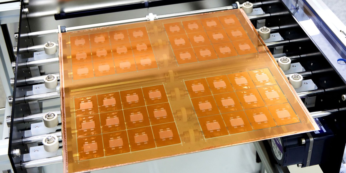
COURTESY OF ABSOLICS INC
Now Absolics is moving toward commercialization; it plans to start manufacturing small quantities of glass substrates for customers this year. The company has led the way in commercializing glass substrates, says Yongwon Lee, a research engineer at Georgia Tech who is not directly involved in the commercial partnership with Absolics.
Absolics says its facility can currently produce a maximum of 12,000 square meters of glass panels a year. That’s enough, Lee estimates, to provide glass substrates for between 2 million and 3 million chip packages the size of Nvidia’s H100 GPU.
But the company isn’t alone. Lee says that multiple large manufacturers, including Samsung Electronics, Samsung Electro-Mechanics, and LG Innotek, have “significantly accelerated” their research and pilot production efforts in glass packaging over the past year. “This trend suggests that the glass substrate ecosystem is evolving from a single early mover to a broader industrial race,” he says.
24World Media does not take any responsibility of the information you see on this page. The content this page contains is from independent third-party content provider. If you have any concerns regarding the content, please free to write us here: contact@24worldmedia.com